UPDI Explained: The Complete Guide to Programming and Debugging Modern AVR Microcontrollers
A comprehensive guide to the Unified Program and Debug Interface (UPDI), including architecture, signalling, security, memory programming, debugging, recovery techniques and programmers.
Table of Contents
- Introduction
- Evolution of AVR Programming Interfaces
- What Makes UPDI Different?
- Physical Layer Architecture
- UPDI Frame Format
- Autobaud Detection
- Session Initialization
- Security Architecture
- UPDI Instructions
- Memory Programming Workflow
- The NVM Controller
- Debugging Through UPDI
- High Voltage Recovery
- Software Tools
- Advantages of UPDI
- Future of AVR Development
- Conclusion
Introduction
The Unified Program and Debug Interface (UPDI) is the programming and debugging backbone of modern AVR microcontrollers. Introduced by Microchip Technology (formerly Atmel), UPDI replaces older interfaces such as ISP, PDI and debugWIRE with a single-wire solution that dramatically simplifies hardware design while maintaining powerful programming and debugging capabilities.
Today, UPDI is used across a growing range of AVR devices, including tinyAVR 0-series, 1-series and 2-series devices, megaAVR 0-series devices and AVR DA, DB, DD and EA families.
For embedded systems engineers, understanding UPDI provides valuable insight into how modern AVR devices are programmed, secured, debugged and recovered. It also opens the door to creating custom programmers, production test fixtures and automated firmware deployment tools.
The Evolution of AVR Programming Interfaces
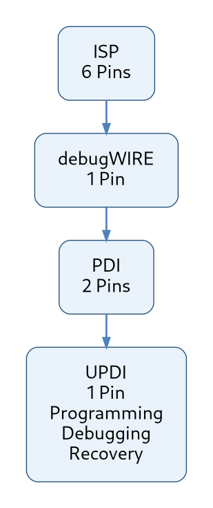
Before UPDI, AVR microcontrollers relied on several different programming interfaces.
In-System Programming (ISP)
Traditional AVR devices such as the ATmega328P used SPI-based In-System Programming.
- MOSI
- MISO
- SCK
- RESET
- GND
- VCC
While effective, ISP consumed valuable pins and increased connector complexity.
JTAG interface
Larger AVR devices often included a JTAG interface for boundary-scan testing and debugging 40 or more pins.
JTAG provided advanced debugging features but required a six-pin connector and additional board space.
For many small devices, JTAG was overkill and impractical.
The need for a simpler, lower-pin-count solution led to the development of debugWIRE and PDI.
debugWIRE
debugWIRE attempted to reduce pin count by using a single-wire debugging interface on the RESET pin.
Although useful for debugging, it was limited in functionality and occasionally cumbersome to recover from.
Program and Debug Interface (PDI)
The XMEGA family introduced PDI.
Microchip eventually unified these approaches into a single protocol:
Unified Program and Debug Interface (UPDI)
The result was a simpler, more flexible solution that reduced hardware complexity while retaining advanced debugging and memory access features.
What Makes UPDI Different?
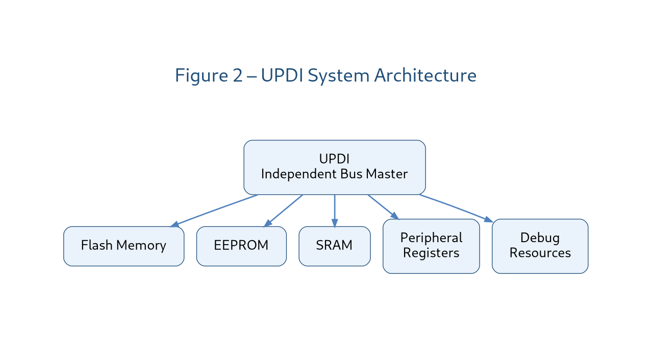
UPDI is fundamentally different from traditional programming interfaces because it operates as an independent bus master inside the target microcontroller.
Rather than interacting solely with the CPU core, UPDI can directly access:
- Flash memory
- EEPROM
- SRAM
- Peripheral registers
- Configuration fuses
- Debug resources
This means UPDI can inspect and modify memory regardless of what the CPU is currently doing.
In many cases, programming operations occur while the CPU is held in reset or completely halted.
This architecture makes UPDI exceptionally powerful compared with traditional bootloader-based programming approaches.
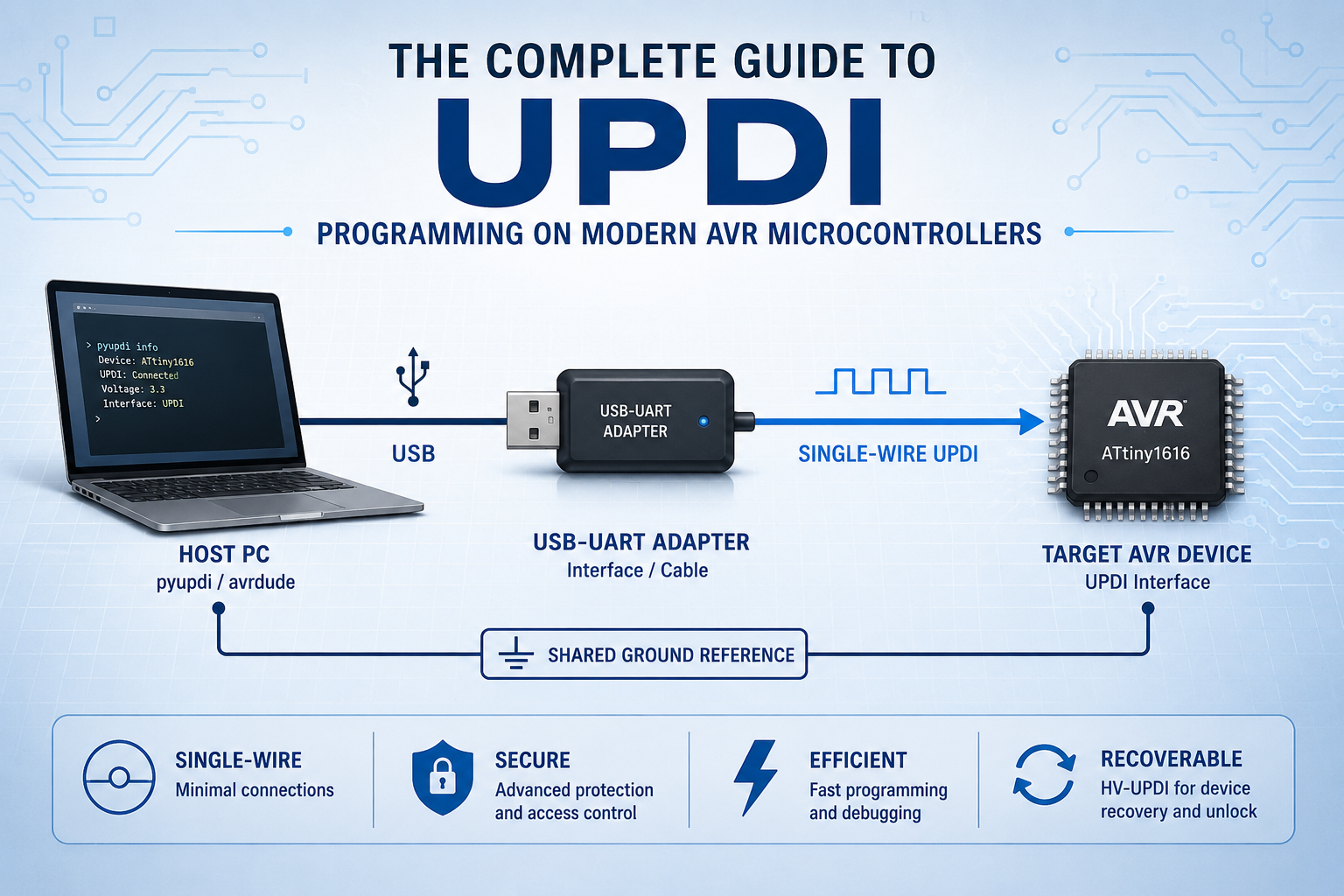
Physical Layer Architecture
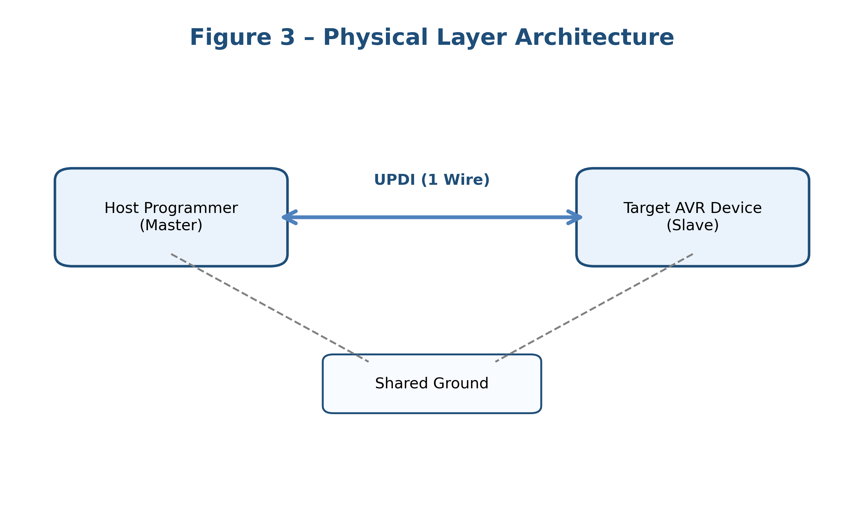
One of the most attractive aspects of UPDI is its simplicity.
- One data wire
- One ground connection
The UPDI pin serves as a bidirectional communication channel between the host programmer and the target AVR device.
Communication occurs in half-duplex mode, meaning only one side transmits at a time.
Idle State
When no communication is occurring:
- The UPDI line remains HIGH
- An internal pull-up resistor maintains the idle state
This creates a simple open-drain style bus architecture.
UPDI Frame Format
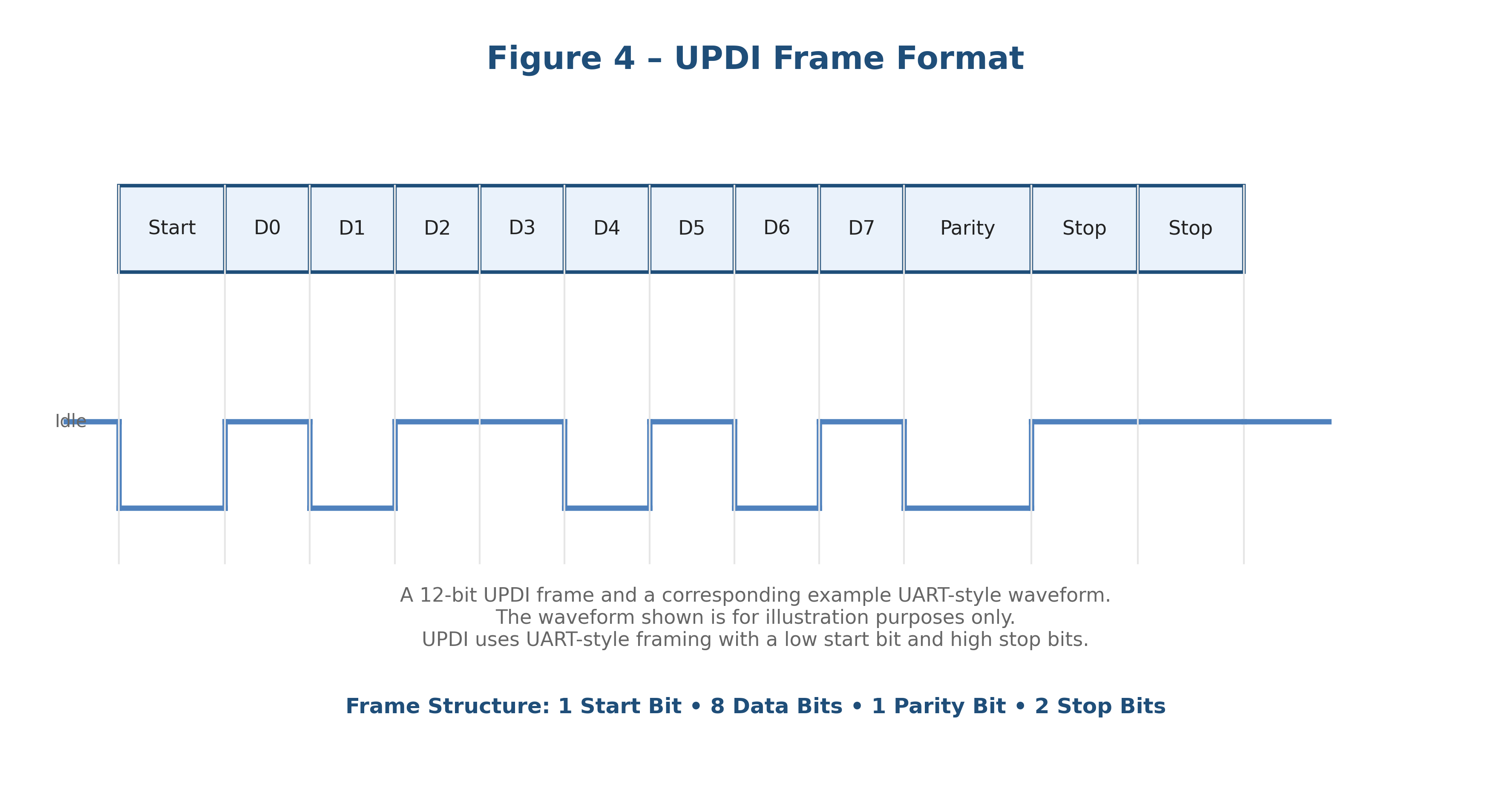
At the protocol level, UPDI uses standard asynchronous UART-style communication.
Each frame contains exactly twelve bits.
| Field | Bits |
|---|---|
| Start Bit | 1 |
| Data Bits | 8 |
| Parity Bit | 1 |
| Stop Bits | 2 |
Data characteristics:
- Least Significant Bit first
- Even parity
- Two stop bits
Example transmission:
| Start | D0 | D1 | D2 | D3 | D4 | D5 | D6 | D7 | Parity | Stop | Stop |This UART-compatible design significantly simplifies implementation. Many developers are surprised to discover that UPDI can be implemented using nothing more than a standard USB-to-UART adapter and appropriate software.
Autobaud Detection
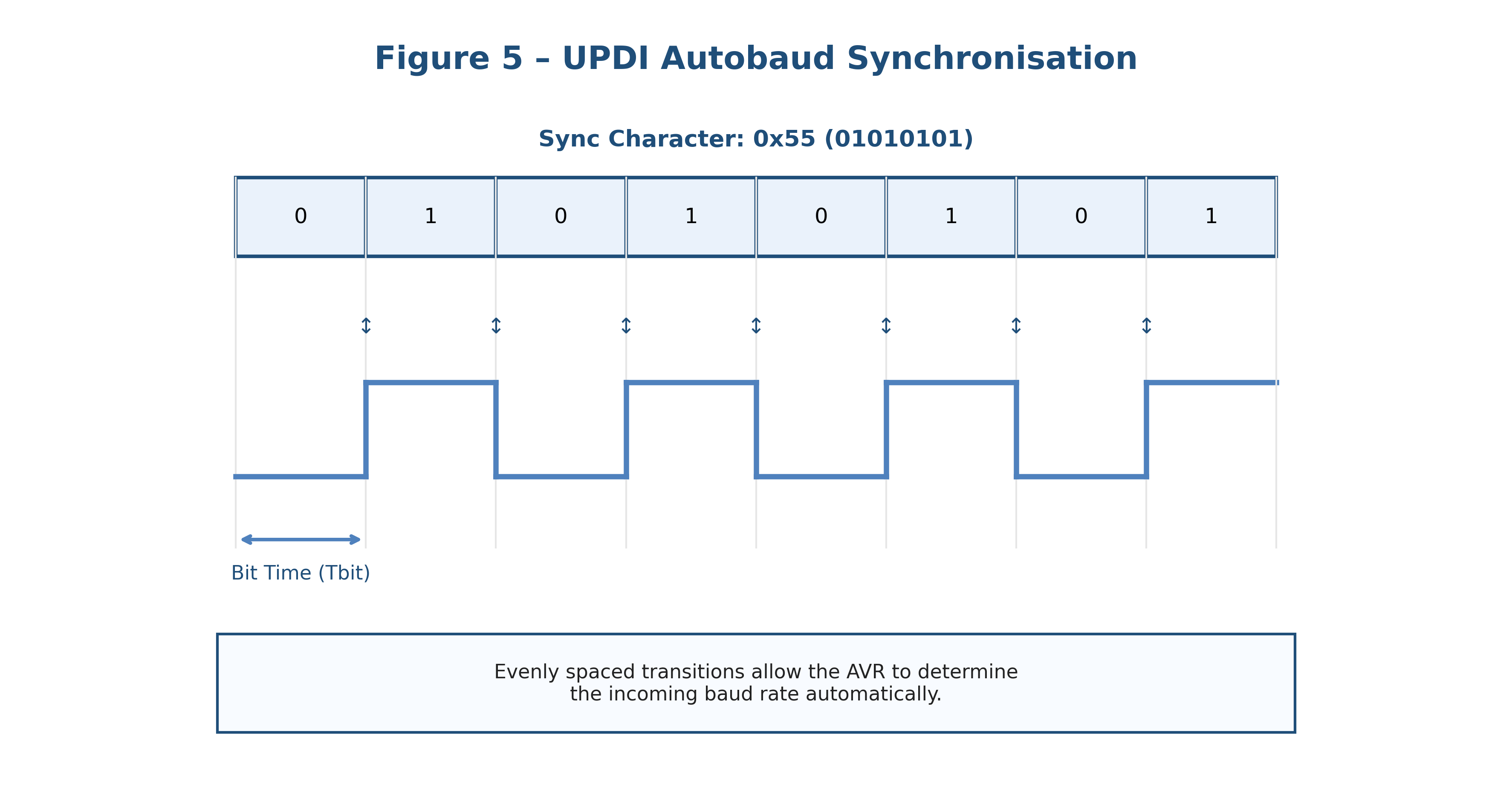
Unlike SPI, UPDI does not provide a clock line. Instead, the protocol uses autobaud synchronization.
The Synchronization Character
The programmer transmits:
0x55Binary:
01010101The alternating bit pattern generates multiple signal transitions. The target device measures these transitions and automatically configures its internal baud-rate generator.
This allows communication without requiring both sides to agree on a fixed clock speed beforehand.
Advantages include:
- Reduced hardware complexity
- Greater flexibility
- Automatic adaptation to oscillator tolerances
- Simplified startup procedures
Session Initialization
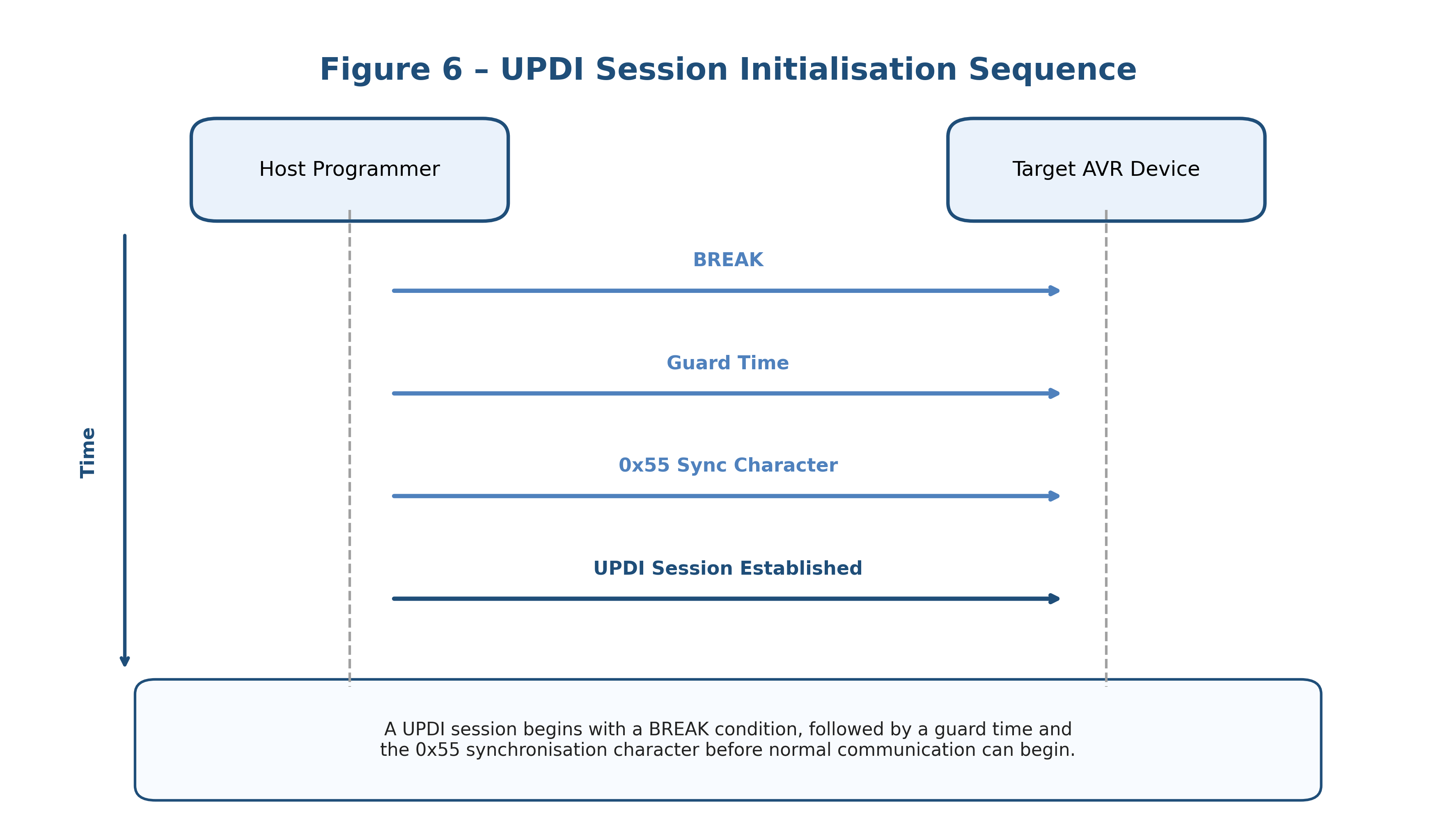
Before programming can begin, the UPDI peripheral must be initialized. The process follows a strict sequence.
BREAK Condition
The programmer first forces the UPDI line LOW.
HIGH ─────┐                     ┌─────
          │                     │
LOW       └─────────────────────┘
This extended LOW period is called a BREAK condition.
The BREAK pulse:
- Resets the UPDI state machine
- Clears communication errors
- Wakes sleeping devices
- Forces synchronization recovery
The pulse duration must exceed a normal frame length.
Guard Time
- The programmer releases the line.
- The pull-up resistor restores HIGH.
- A brief delay allows stabilization.
Only after this guard interval may communication continue.
Synchronization
The programmer sends:
0x55The target performs autobaud calibration and communication is established.
Security Architecture
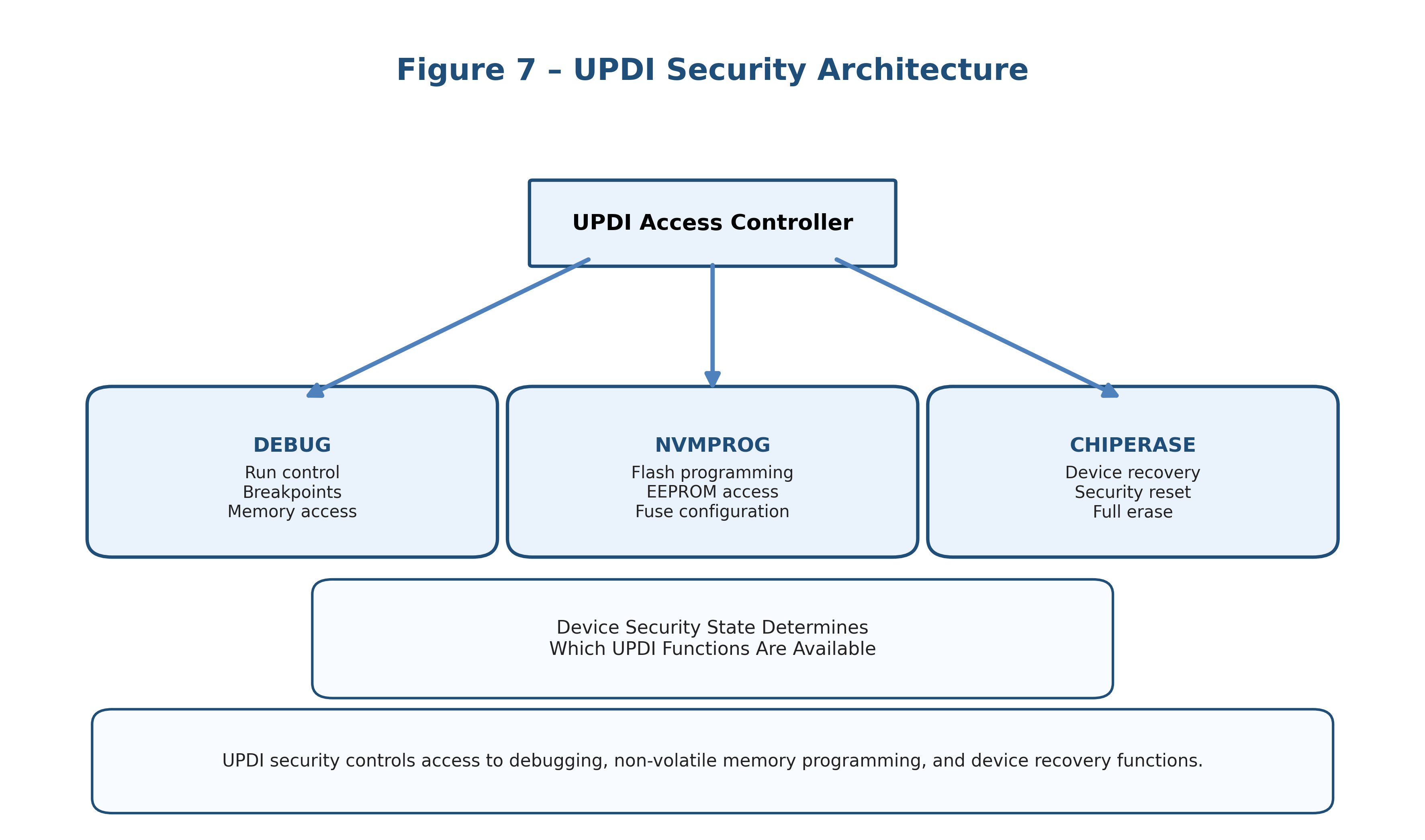
Modern AVR devices incorporate robust security mechanisms.
These protections prevent:
- Unauthorized firmware extraction
- Accidental memory corruption
- Unauthorized debugging access
UPDI controls access through cryptographic-style activation keys.
Programming Key
The NVMPROG key enables:
- Flash programming
- EEPROM access
- Fuse modification
Debug Key
The DEBUG key enables:
- Breakpoints
- Register inspection
- Runtime debugging
Chip Erase Key
The CHIPERASE key performs a complete device erase. This operation is often required before access can be restored to a secured device.
Understanding UPDI Instructions
The UPDI instruction set is surprisingly compact. Rather than implementing high-level commands such as “Program Flash”, UPDI provides primitive memory access operations. Everything else is built on top of those operations.
Direct Memory Access Instructions
LDS
Load Data from Direct Address
Reads a byte from a specified memory location.
Read address 0x1000
Return byte value
STS
Store Data to Direct Address
Writes a byte to a specific memory address.
Write 0x55 to address 0x1000
Pointer-Based Access
For large transfers, repeatedly specifying addresses becomes inefficient. UPDI solves this with pointer-based instructions.
LD
Load via Pointer. The internal pointer specifies the memory location and optional auto-increment allows burst reads.
ST
Store via Pointer. Auto-increment enables efficient streaming and is heavily used during Flash programming.
Control and Status Registers
UPDI contains internal control registers separate from the AVR memory map.
LDCS
Load Control and Status.
STCS
Store Control and Status.
These registers control:
- Configuration
- Status reporting
- Security state
- Reset behavior
Memory Programming Workflow
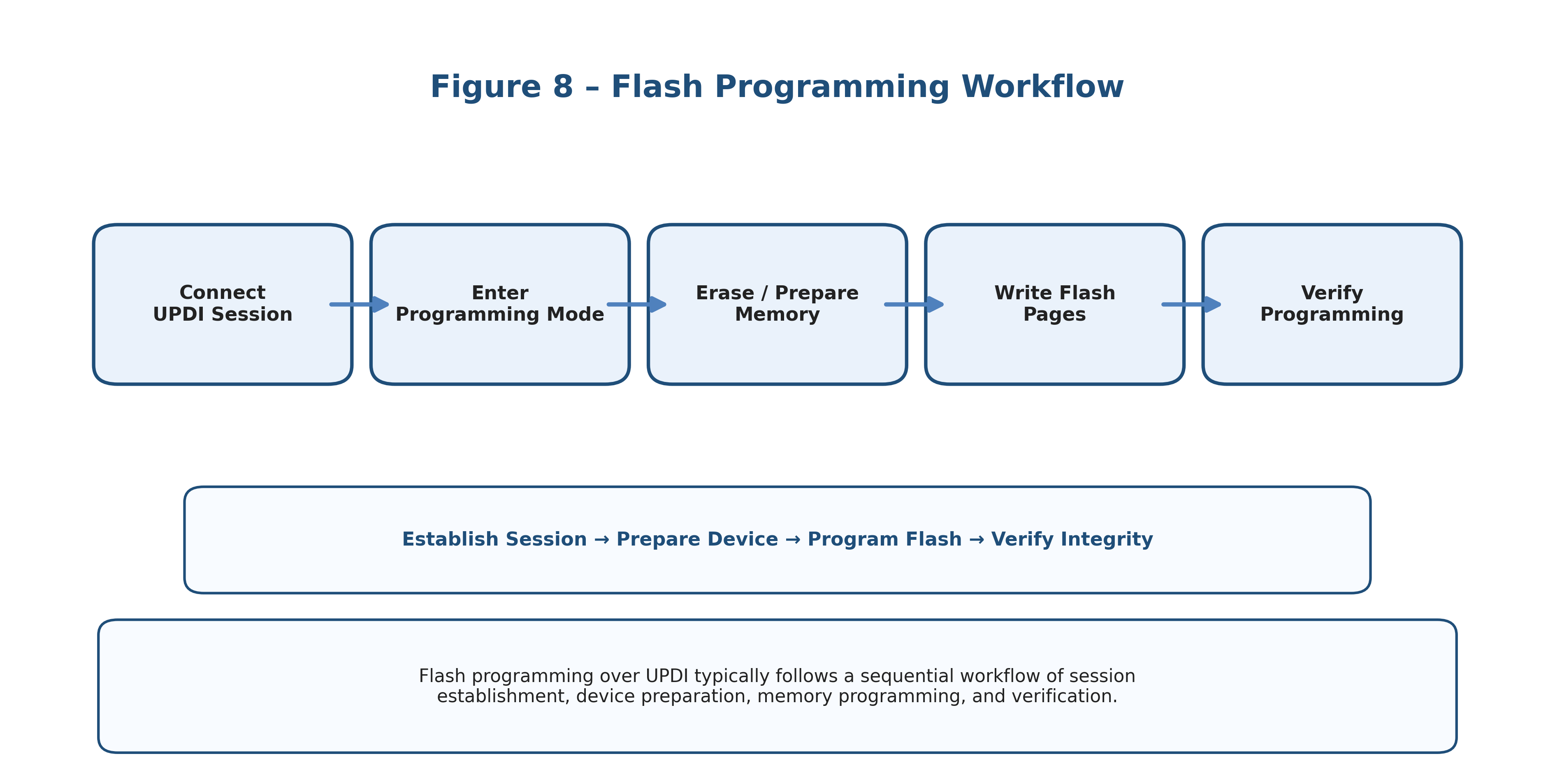
Programming Flash memory involves significantly more than simply writing bytes.
A typical flash programming sequence is shown below:
- Enable programming mode and establish an active UPDI session.
- Verify key acceptance and confirm that programming access has been granted.
- Reset the CPU core to place the device in a known state.
- Configure the NVM controller for the required programming operation.
- Load the page buffer with the new firmware data.
- Execute the page write operation and allow the NVM controller to perform erase/program cycles.
- Verify programmed contents to ensure memory integrity.
- Release reset and return control to the application.
- Start application execution and resume normal operation.
Commercial tools such as MPLAB Snap, PICkit and Atmel-ICE perform these operations automatically.
The NVM Controller
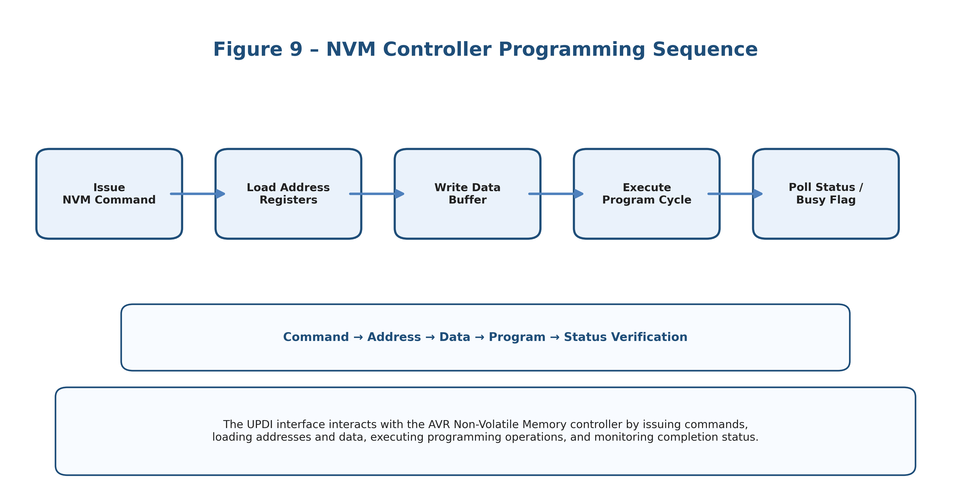
Modern AVR devices contain dedicated hardware for Flash programming.
The NVM controller handles:
- Page buffering
- Erase operations
- Flash programming
- Verification
Direct writes to Flash cells are impossible.
Instead:
- Data enters a page buffer.
- The controller performs erase/program cycles.
- Flash contents are updated atomically.
This protects memory integrity and improves reliability.
Debugging Through UPDI
UPDI is not merely a programming interface.
It also provides debugging functionality.
Available features often include:
- Hardware breakpoints
- Single-step execution
- Register inspection
- Memory examination
- Runtime control
Because the debugger communicates directly through UPDI, no additional debugging connector is required.
High Voltage UPDI Recovery
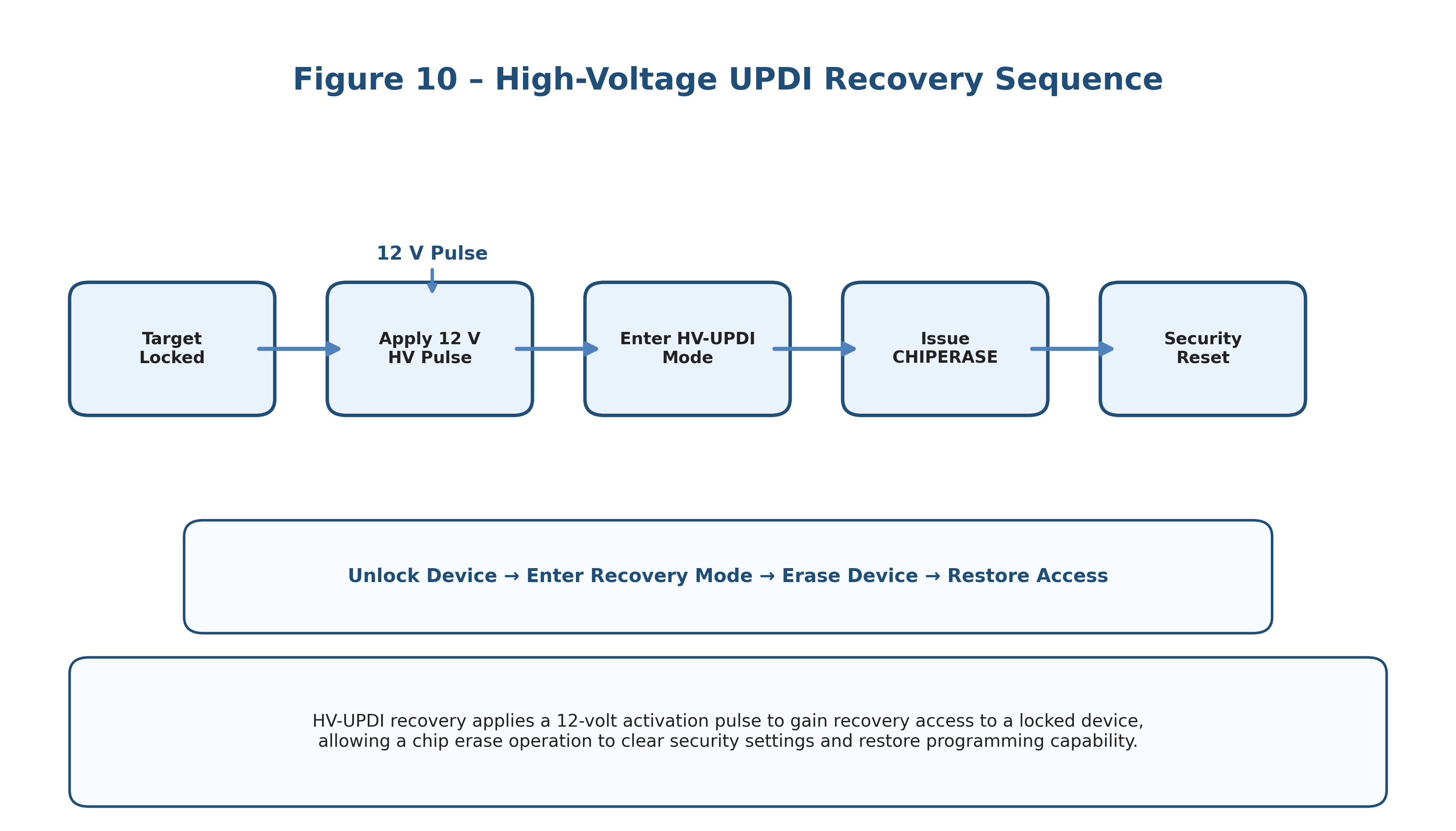
One common mistake is disabling UPDI through fuse configuration.
Historically, this could permanently lock a device.
Modern AVR devices solve this problem using High Voltage UPDI (HV-UPDI).
A high-voltage pulse temporarily reactivates the programming interface.
Once activated:
- UPDI becomes available again.
- A valid key sequence is transmitted.
- Recovery operations can proceed.
This feature significantly reduces the risk of accidentally “bricking” a device.
Popular UPDI Software Tools for Debugging your code
- avrdude
- Widely used command-line programmer supporting many third-party UPDI adapters.
- pymcuprog
- Microchip’s Python-based programming framework providing direct access to UPDI functionality.
- SerialUPDI
- Open-source implementation using inexpensive USB-UART adapters and widely used by hobbyists and makers.
- MPLAB X
- Microchip’s integrated development environment providing full programming and debugging support.
Advantages of UPDI
- Reduced Pin Count – Only a single signal line is required for programming and debugging.
- Lower Cost – Fewer pins mean smaller connectors, reduced PCB routing and simpler hardware.
- Easier Manufacturing – Production fixtures become simpler, more robust and easier to automate.
- Advanced Debugging – Programming and debugging share the same physical interface.
- High Performance – Burst memory operations allow efficient firmware programming.
- Strong Security – Key-based access mechanisms help protect device contents and debugging resources.
Future of AVR Development
UPDI has become the standard interface across Microchip’s modern AVR ecosystem.
As newer families continue to appear, developers can expect UPDI to remain central to:
- Firmware deployment
- Production programming
- Device recovery
- Debugging workflows
- Automated manufacturing systems
Its combination of simplicity and capability makes it one of the most elegant programming interfaces available in the embedded world.
Conclusion
The Unified Program and Debug Interface represents a major evolution in AVR development technology.
By combining a single-wire physical layer with direct memory access, integrated debugging, autobaud synchronization and built-in security mechanisms, UPDI delivers a powerful yet surprisingly simple solution for modern microcontroller programming.
Whether you are developing a custom programmer, designing a production fixture, reverse-engineering AVR communication or simply programming your first tinyAVR device, understanding UPDI provides valuable insight into the architecture that powers modern AVR development.
For embedded engineers, UPDI is more than a programming connector—it is a direct gateway into the heart of the microcontroller itself.